High-quality vacuum solutions for the hightech industry
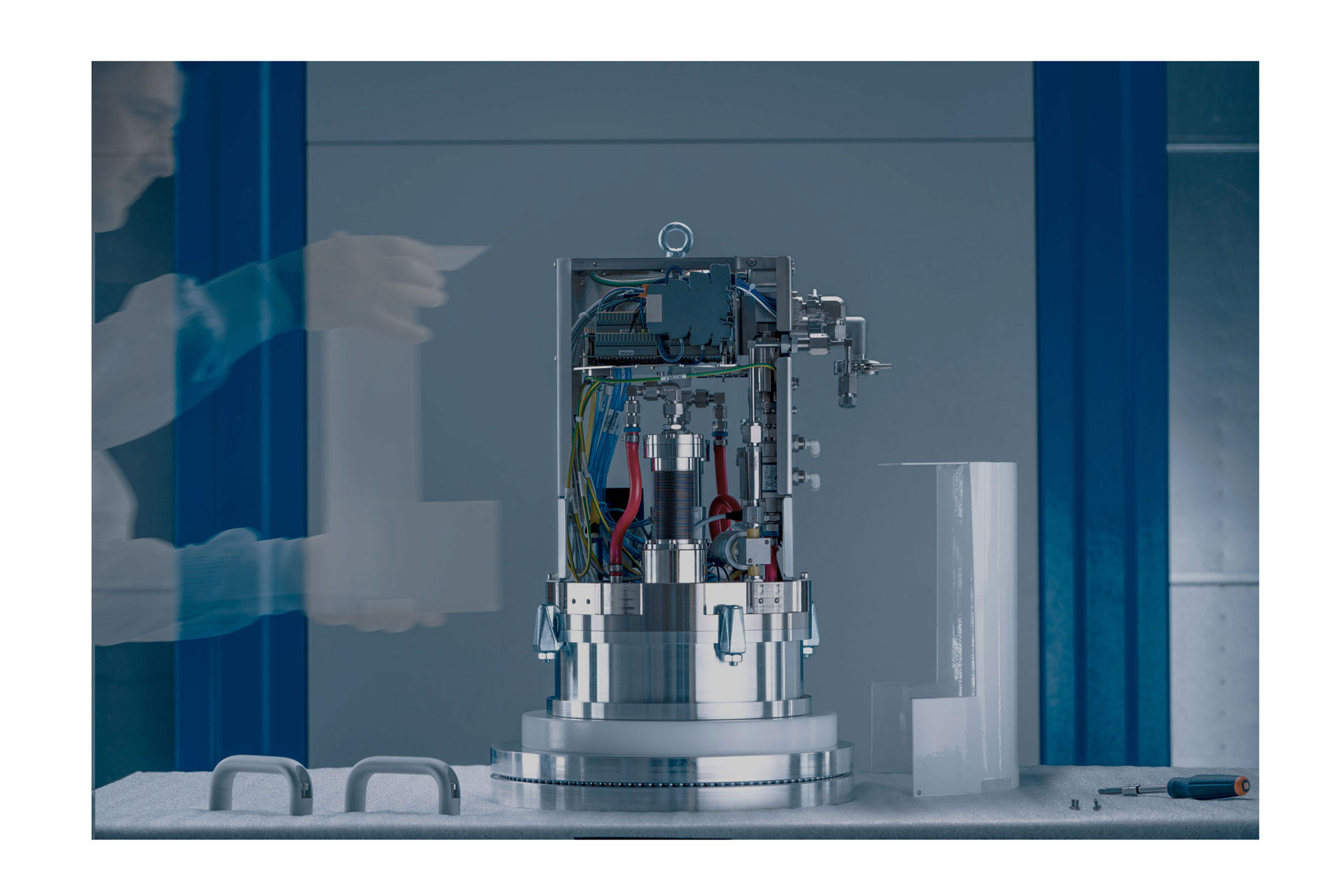
As a leading system supplier in highvacuum technology, we serve the semiconductor, coating and R&D markets as well as the manufacturers of analysis and treatment devices. We stand for innovative solutions, hightech and reliable products as well as first-class service. With experience, knowhow and constant innovative strength, we cover a wide range: from standard flanges to complete assemblies, to hermetically sealed electrical and optic feedthroughs, edge-welded housings and vacuum chambers.
The elements we manufacture are standard components in vacuum production, coating and research systems. These systems are becoming more and more complex and the demands on the sealing technologies are increasing. Our processes are constantly being further developed in order to actively support our customers’ innovation projects. A special focus is on the joining technology.
Fields of application: Analytical devices, coating systems, chips
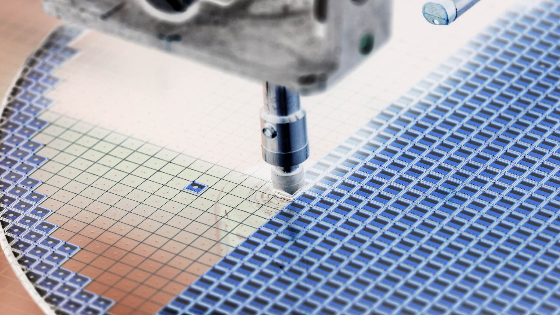
Our products are also used in vacuum evaporation machines and thin film coating process systems. The innovative coating techniques are used in the production of wafers – so-called semiconductor discs. The layers of the wafers filter colors and frequencies, pass on signals or block them. They provide diverse functionality in the smallest of spaces; therefore the resulting components are extremely small and this is an important USP in the telecommunications, semiconductor and solar industries.
A number of the thinly coated, multifunctional components are found in smartphones, for example. Our customers are champions when it comes to developing the layers and building the systems with which the components are manufactured.

We master the visions of the future
We also supply the world market leaders in mechanical engineering for the production of super microchips. In a cross-company working group, one of the currently most modern systems was developed: a wafer scanner for EUV lithography, which is the semiconductor production with extreme ultraviolet light. The hightech unit weighs 180 tons and costs around 120 million euros. Laser technology plays a central role: it generates EUV light, which can be used to produce much more powerful chips. Inside the machine, these light beams etch nanometer-sized structures on silicon discs in a vacuum chamber – the basis for transistors, which ultimately form a microchip.
The purpose is to make the chips even smaller and even faster than they already are. They are needed to create virtual realities, to awaken artificial intelligence, to build networked factories, and to make full use of the potential of Big Data or the 5G wireless standard. Smartphones are becoming more and more powerful, their functions get more and more diverse, with quite the same size.

Real-time analysis methods
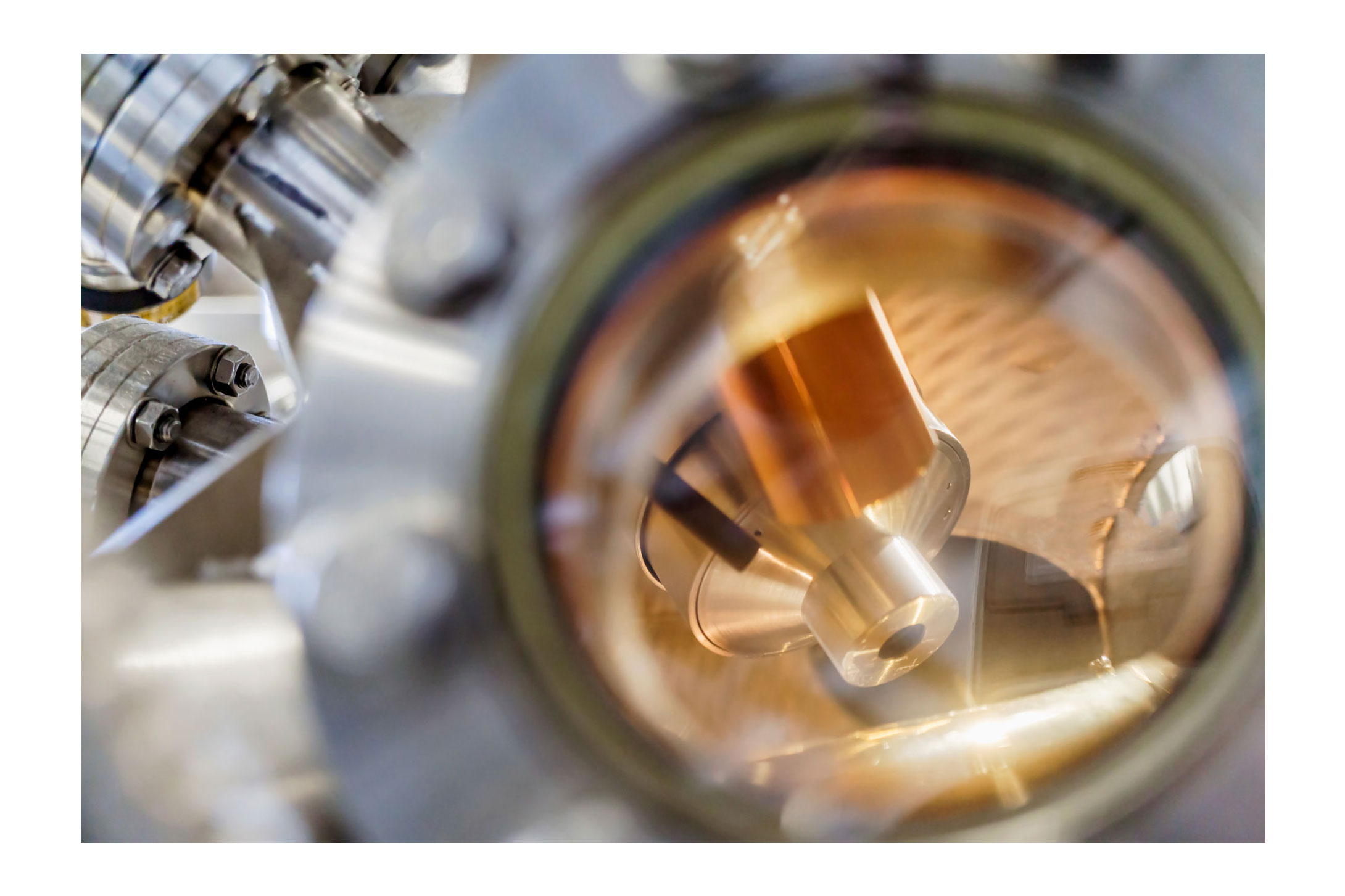
Another area of application for our products is in the field of analytical instruments, for example electron microscopy and mass spectrometry. Especially in biotechnology, real-time analysis methods are critical to success due to time and cost reasons. Chemists use the method to analyze chemical elements and compounds. It is possible, for example, to detect very small amounts of substance in samples.
The method is correspondingly popular with toxicologists, who can detect poisoning and drugs in the blood; the same goes for environmental chemists who discover pollutants in soil samples. Biologists, on the other hand, use mass spectrometry to study proteins in living things. Physicists determine the mass of atomic nuclei. And archaeologists analyze isotope ratios in human bones and thus draw conclusions about their diet. The technology is now even being used at airports to detect residues of explosives or drugs on passengers and luggage.


